
TNO warns: Europe's electronics window is closing fast
TNO says Europe must shift from chip-making to system integration to stay relevant as AI reshapes electronics architecture.
Published on September 2, 2026
© TNO

Team IO+ selects and features the most important news stories on innovation and technology, carefully curated by our editors.
Dutch research organisation TNO has published a new paper arguing that the electronics industry is entering a fundamental architectural shift, one that could redraw the map of technological power in the coming decade. And Europe needs to move fast to secure a place in it.
The paper, titled Beyond PCB and Chips: The Invisible Revolution in Electronics and the Opportunities for Europe, contends that by 2035 electronics will no longer advance mainly through more connected devices, but by becoming an invisible, intelligent layer woven into machines, infrastructure and everyday environments. TNO likens this to how electricity and internet connectivity once became transformative only after they receded into the background of daily life.
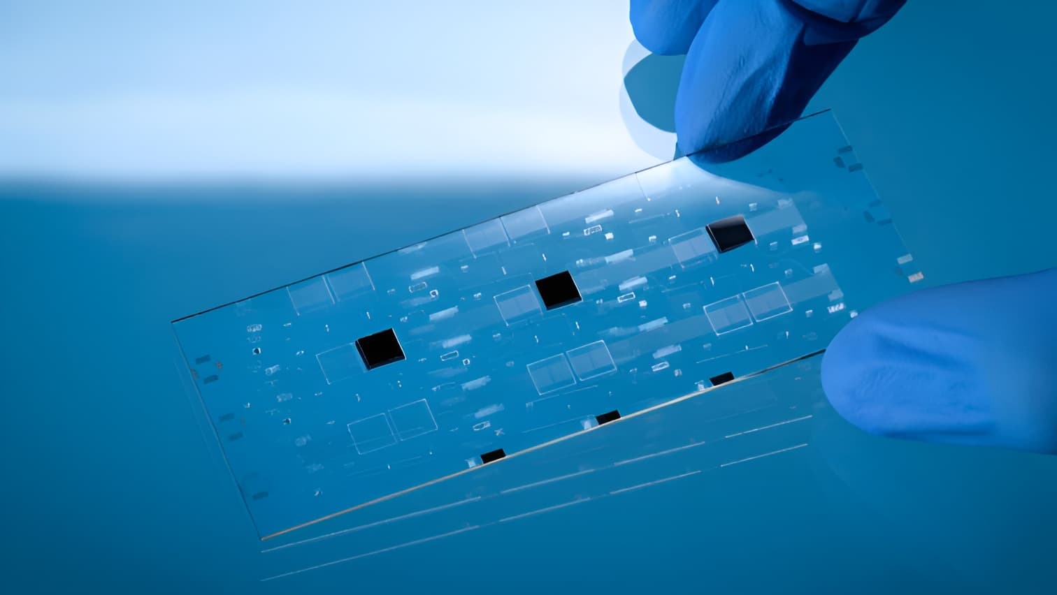
The driving force behind this shift, according to the paper, is artificial intelligence. AI training and inference are pushing traditional printed circuit boards (PCBs) and single, monolithic chips beyond their practical limits. As data rates climb, copper interconnects become increasingly costly in energy per bit, and each additional PCB layer or connector adds loss, cost and risk of failure. The result, TNO argues, is a decisive relocation of complexity away from boards and single chips toward the package level, where multiple chiplets, memory, sensors and photonic elements are combined into tightly integrated, purpose-built assemblies.
The key technologies in this shift
The report identifies three converging technologies underpinning this transition: integrated photonics, which uses light rather than electrical signals to move data more efficiently as it is pulled ever closer to the chip itself; advanced chip packaging, which the authors describe as becoming "the system" in electrical, optical, thermal and mechanical terms; and so-called "Beyond PCB" integration, which splits into two paths — one driven by high-performance computing needs, the other by flexible, printed electronics for wearables, smart packaging and large-area sensors.
TNO also frames sustainability as a structural design constraint rather than an afterthought, warning that scaling today's electronics paradigm to a future "trillion-sensor economy" would otherwise multiply material use, energy consumption and e-waste. Concentrating functionality into fewer, highly integrated components is presented as key to avoiding that outcome.
Capturing tech control points
Strategically, the paper echoes the EU's post-Draghi competitiveness agenda, arguing that Europe's future influence will not come from chasing full self-sufficiency in chip manufacturing, but from capturing indispensable "control points" in system integration — areas such as advanced packaging, photonic interconnects, and testing and metrology for heterogeneous systems. TNO points to existing Dutch strengths in these fields, spread across technology hubs in Eindhoven, Twente, and the Arnhem/Nijmegen region, involving companies and institutes such as Nexperia, NXP, Besi, Smart Photonics and TU Eindhoven.
The paper closes with a policy roadmap urging Dutch and European authorities to address fragmented value chains, close the gap between pilot-scale R&D and industrial manufacturing, and create stronger lead markets — including through defence procurement — to help translate research strengths into durable industrial positions before the window for doing so closes.