New chip pilot line aims to deliver on Europe’s tech sovereignty
A €2.5B pilot line is now live at imec, promising to put Europe at the forefront of next-gen chip development.
Published on February 10, 2026
© imec

Mauro swapped Sardinia for Eindhoven and has been an IO+ editor for 3 years. As a GREEN+ expert, he covers the energy transition with data-driven stories.
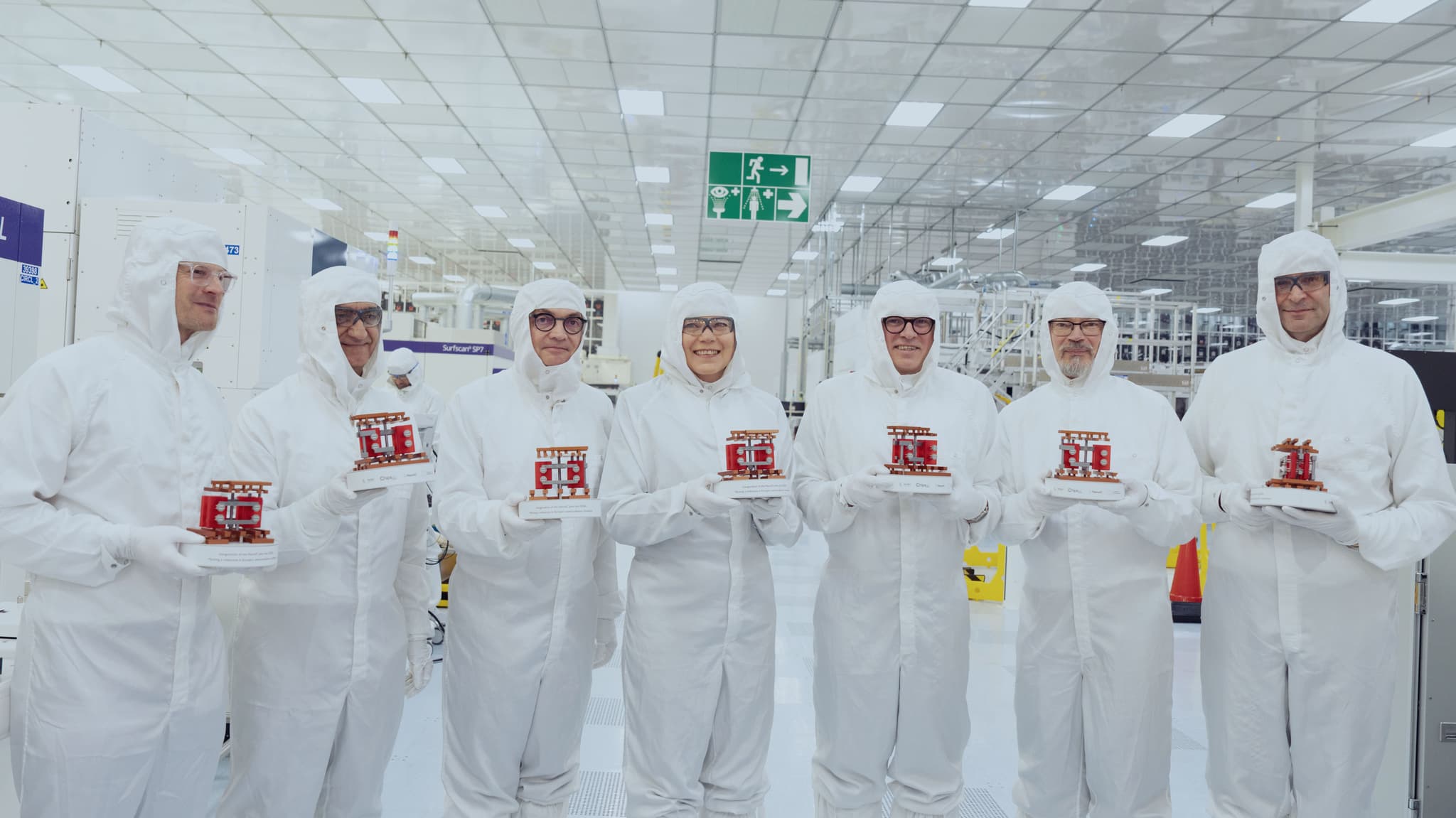
Exactly four years after announcing the European Chips Act, its largest chipmaking pilot line has been inaugurated. The NanoIC Pilot line, housed at Belgium microelectronics research center imec in Leuven, will serve to test and develop the future breakthroughs in chip technology. Reporter Mauro Mereu from IO+ was present at the opening.
The pilot line is backed by a €2.5 billion investment, with contributions from the European Union, the Flemish government, and chipmaking equipment manufacturer ASML. The project is one of the strategic initiatives supported under the European Chips Act, a plan to boost Europe’s semiconductor sovereignty and competitiveness.
“This facility, an extension of our production line, helps reinforce our leadership in semiconductor technology research and development,” stated on stage imec’s CEO, Luc Van den hove. Facilities like the new pilot line are beneficial and create “reverse dependencies” on Europe—rather than on third countries—emphasized Van den hove.
The line has come into life in a 3000 m2 cleanroom, featuring some of the most advanced chipmaking machinery. The facility is open to everyone, from established companies to startups, to test new chip designs before they go into mass production.
Printing components 40 times smaller than a human hair
The pilot line is a large, white, cleanroom. Given the machinery's high sensitivity to dust, operators wear lab coats, boots, and gloves. An aeration system is in place to continuously recirculate airflow. The line is designed to enable sub-2-nanometer (2nm) systems-on-a-chip (SoC) technology. For comparison, a human hair is approximately 80 nm in diameter.
Developing smaller nodes means more transistors—semiconductors’ fundamental building blocks—can fit into the same space, enabling faster chips—transistors can switch at higher speeds—greater energy efficiency, and more complex designs. A 2nm node can include 300 transistors per square millimeter, supporting heavy computing tasks.
The smaller, the more powerful
Scaling down chip components' size is the industry leitmotif. Over the past decade, SoC size has shrunk from 14 nm to 2nm today. While smaller chips can serve a range of technology areas, from connectivity to personalized medicine, they deliver the greatest benefits for AI development. In particular, they enable AI integration across a range of devices, from smartphones to cars.
Chip manufacturers are beginning to mass-produce 2nm platforms. Chipmaker TSMC has begun mass production of 2nm wafers. Apple is among the first customers and will integrate the tiny chips into the upcoming iPhone 18 series, which launches later this year. Samsung is also ramping up production.
Going beyond the 2nm scale means unlocking new possibilities and forcing further technological breakthroughs.
ASML’s involvement
ASML has committed over €1 billion of the investment needed for the NanoIC line. Among the platform's top-tier machinery, ASML’s narrow-aperture (NA) extreme ultraviolet (EUV) machine will be installed by March.
Christophe Fouquet, CEO of the chipmaking equipment company, praised imec for its long-standing collaboration with ASML, noting that the Belgian institute “was the first to believe in our technology.”
In his address, the leader underscored the necessity to scale up on semiconductor production technology and capabilities. “Every innovation will have an AI prominence,” he stated. “By 2030, we will reach the billion threshold of transistors on a chip. This proves how fast we need to go in order to accommodate the needs AI development entails.”
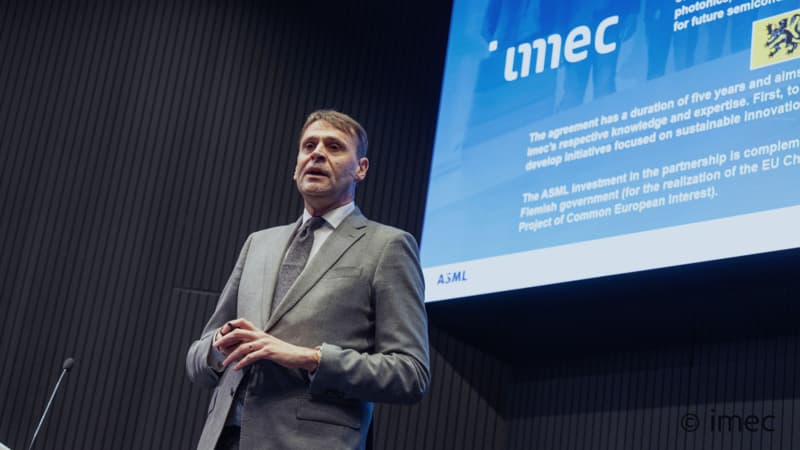
Christophe Fouquet speaking at the inauguration event - © imec
Building on European excellence
By no coincidence, the largest pilot line is housed at imec. The institute has been spearheading microelectronics research for decades, building a tight-knit network with industry leaders. The relationship with ASML is particularly significant and has been reinforced with a partnership agreement last year.
According to imec’s CEO, Luc Van den hove, Europe must keep building on its strengths. “Europe needs to cement its strengths to reinforce itself, connecting excellences, rather than competing against each other.”
Belgian Prime Minister Bart De Wever echoed him, underscoring that Europe should double down on what it excels at, rather than pursuing technologies it lacks leadership on. In a shifting geopolitical order where the Old Continent isn’t as influential, the direction should be different. ”Europe must exert smart power, building the technology the world can’t build.”
Chip Act 2.0 is coming
ASML and imec epitomize Europe’s excellence, as their scientific research often doesn’t translate into impactful technology. Executive Vice-President for Tech Sovereignty, Security and Democracy Henna Virkkunen, also present at the NanoIC inauguration, stressed how “bridging the gap from lab to fab” was one of the Chips Act's main goals. The regulation also aimed to help the EU retain 20% of the global semiconductor market by 2030—double its 2022 share.
Speaking on stage, the official announced that the Chips Act 2.0 is on the way to address the gaps of the previous legislation. “Addressing the supply chain resiliency will be one of the priorities,” told IO+ Virkunnen.
“Global supply chains proved to be extremely vulnerable, and even a small disruption can cause major damage. At the same time, if we want to design and produce the best chips in the world, we need to make our excellence collaborate further,” she added.

A moment of Virkkunen's speech © imec
The virtuous cycle of fueling innovation
There is no economic prosperity for Europe without innovation and technological progress; that’s the main message that resonates from imec’s auditorium stage. Doing so means building on strengths and uniting forces and knowledge across member states.
The NanoIC pilot line is a cross-border collaboration among institutions across the bloc, including CEA-Leti (France), Fraunhofer (Germany), VTT (Finland), CSSNT (Romania), and Tyndall National Institute (Ireland).
As the world digitalizes and progressively embraces AI, the semiconductor industry is a matter of geopolitical interests, technological sovereignty, and strategic autonomy. Being at the forefront of these developments is key. ASML and imec know it well; officials seem to have learned the hard way, too.
There is no time to catch a break; competition from East and West is fierce. To remain relevant and competitive, Europe must continue to fuel innovation. The NanoIC Pilot line aims to deliver on this promise.