New advanced applied research lab is a photonics playground
At the Holst Centre Photonics Lab, imec and TNO combine forces to accelerate innovation, opening their doors to support third parties.
Published on May 12, 2025
© imec / TNO

Bart, co-founder of Media52 and Professor of Journalism oversees IO+, events, and Laio. A journalist at heart, he keeps writing as many stories as possible.
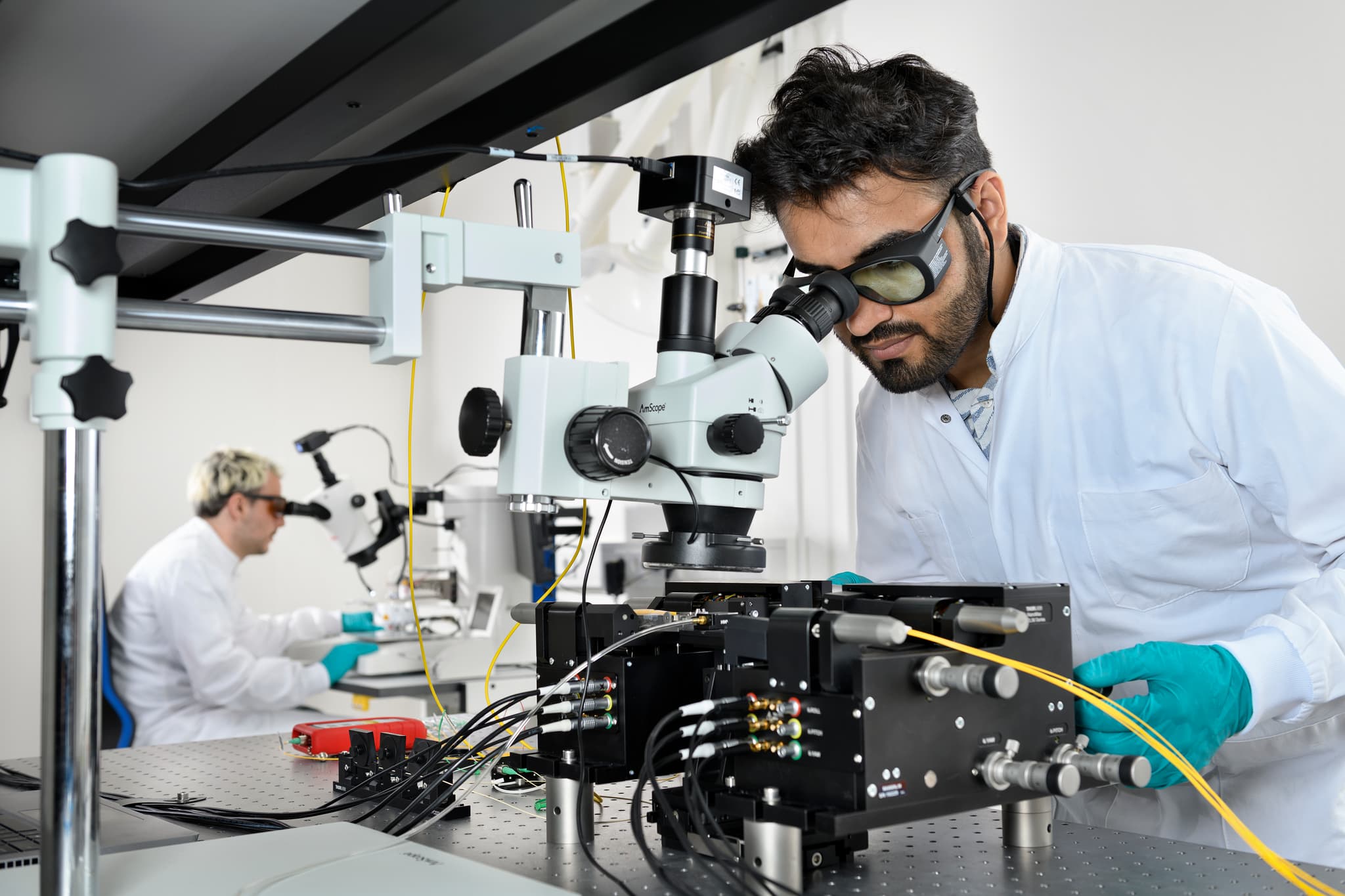
Hidden behind secured glass doors in a hidden corner of Eindhoven’s High Tech Campus lies a brand-new facility with outsized ambitions. The Holst Centre Photonics Lab, jointly developed by research powerhouses imec and TNO, is now fully operational. It's the only applied photonics lab in the Netherlands operating on this scale, designed not just for cutting-edge internal R&D, but also to support startups eager to test, validate, and scale photonic innovations.
“This laboratory is the only one in the Netherlands for applied research on this scale,” says Ruud Oldenbeuving, chief scientist of photonics at imec. He gestures toward a row of high-precision instruments used to develop and test photonic chips. “We’ve built this to accelerate the entire innovation chain, from chip design to packaging, from concept to application.”
At the heart of the lab’s mission is integrated photonics, with immediate focus areas like LiDAR for autonomous driving, next-generation healthcare sensors, and ultra-fast optical communication. Photonic chips - faster, smaller, and more energy-efficient than their electronic counterparts - are expected to transform these fields. But to do that, they need to be not only well-designed, but well-packaged, tested, and integrated with electronics. That’s where collaboration between imec and TNO comes in.
“Imec brings its expertise in system development and manufacturing,” says Oldenbeuving. “TNO focuses more on packaging, thermal management, and heterogeneous integration. Here, we bring those worlds together.”
Compact power, high impact
One of the lab’s current projects is the miniaturization of LiDAR systems, the laser-based sensors that help autonomous vehicles perceive their surroundings. “Most current LiDAR systems are bulky and expensive,” explains one of imec’s experts. “Our goal is to create a system the size of a credit card, priced under $100. That’s what the automotive sector is demanding.”
To reach that goal, imec researchers are building chips that not only send and receive laser signals but also process the data. “We use the same foundries and fabrication lines as for electronic chips,” adds Oldenbeuving. It's just a different recipe.”
Even more ambitious is the team’s work on LiDAR networks, systems where multiple LiDARs communicate with one another, extending range and sharing data. “It’s not just about detecting objects anymore,” says one of the researchers. “We’re combining LiDAR with high-speed data communication. The same beam that senses can also carry 50 to 100 Gbps of data.”
Healthcare, Reimagined
The lab’s innovations aren’t limited to vehicles and communication. In another corner of the lab, TNO researchers are testing laser-based health sensors that outperform today’s smartwatches, especially for people with darker skin tones. Traditional photoplethysmography (PPG) sensors are often unreliable in those cases, but a speckle-based laser system developed here solves that.
“This method creates a dynamic laser pattern on the skin and measures the changes as blood flows,” explains an imec researcher. “It’s more robust against ambient light and skin tone variation and allows for non-contact, multi-person heart rate monitoring.”
The team is now working on miniaturizing the system for integration into consumer devices. “We’re transitioning from big modules to chip-scale VCSELs and camera units. The Holst Centre Lab makes that transition possible.”
The same speckle-based technique is being explored for agriculture, measuring the sap flow in plants or even the heart rate of cows during milking.
.jpeg&w=2048&q=75)
© imec / TNO
Photonics for the real world
TNO's researchers introduce another breakthrough: glass-based panel integration. “We build modules where photonics and electronics are integrated on a single substrate,” he says. “It reduces cost, improves heat management, and is essential for real-world deployment.”
Packaging is more than an afterthought in photonics; it’s often 80% of the system’s cost. “We’re working on panel-level and wafer-level packaging to reduce costs and boost scalability,” says a TNO expert. “That’s essential for consumer applications.”
Applications like LiFi, the optical alternative to WiFi, are already being demonstrated in the lab. Using light rather than radio waves, LiFi offers secure, jam-resistant communication with vastly more bandwidth. TNO shows a live video stream beamed via a narrow light beam: “We’re designing receivers that can integrate into smartphones and laptops. This is real-time data transfer at 2.5 Gbps.”
Open innovation on a national scale
The Holst Photonics Lab is more than a shared workspace; it’s a national resource. “Thanks to support from PhotonDelta and other partners, we’ve built a facility where others can test their prototypes,” says Oldenbeuving. “Startups that can’t afford a €500,000 instrument can potentially benefit from our facilities, under fair conditions.”
Smart Photonics, Mantispectra, and many younger companies stand to benefit. “There are a lot of specialized players in the Netherlands,” says Oldenbeuving. “But few places where they can bring all the building blocks together.”
The lab closes critical gaps in the photonics innovation chain by uniting design, testing, packaging, and application under one roof. “You can't go from lab demo to market-ready tech without this infrastructure,” says Oldenbeuving. “This is the bridge.”