
Delmic puts nanoscale research on autopilot
Delmic is developing a technology, SPARC 3.0, that makes electron microscopy faster and easier.
Published on September 4, 2026
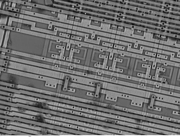
SEM image of microstructures on a wafer.

Our DATA+ expert and Editor-in-Chief, Elcke Vels, explores AI, cyber security, and Dutch innovation. Her "What if..." column imagines bold scenarios beyond the norm.
Whether it involves new chips or processes within our bodies, more and more research is being conducted at the nanoscale. Electron microscopy plays a key role in this field. Delft-based Delmic launched a measurement system earlier this week that automatically performs specialized operations typically carried out by such microscopes. “The plan is to sit down with industrial clients,” says Sander den Hoedt, CEO of Delmic.
Society is increasingly turning to electron microscopy. This technique allows researchers to map processes down to the nanoscale accurately. Roughly speaking, it works like this: an electron beam is directed at a minuscule piece of material, after which the returning electrons provide information about what is happening there on the nanoscale.
What happens on the nanoscale can have major consequences. Take the human body, for example. It consists of countless tiny biological components, such as proteins. If something goes wrong on the nanoscale, diseases can develop, such as Alzheimer’s. It is therefore crucial that researchers be able to take precise measurements, both for basic research and for the development of new medicines.
Electron microscopes play a major role in the life sciences, as well as in materials research and the semiconductor industry. In materials research, for example, they are used to study solar cells or data center components, and in the semiconductor industry to detect defects. Furthermore, when it comes to new semiconductor materials such as gallium nitride and silicon carbide, researchers must not only be able to find defects but also determine how often they occur and under what conditions.
The importance of automation
Delmic aims to make electron microscopy easier and faster. The new measurement system launched on Monday, SPARC 3.0, automatically takes over certain specialized tasks and performs certain measurements up to 2.3 times faster. Den Hoedt: “It’s an ‘add-on,’ so the customer already has an electron microscope, and we install SPARC on it.”
It is precisely this automation that is sorely needed in the world of electron microscopy. Many companies are focused on producing increasingly sharp and detailed images of the nanoworld. According to Den Hoedt, however, that’s not where the biggest challenge lies. “I sometimes joke with people: it’s like putting bigger and bigger engines in Ferraris so they can go 380 kilometers per hour instead of 300. But then that Ferrari sits in traffic all day. We’re solving that traffic jam with SPARC 3.0.” In other words: automation makes electron microscopy more accessible and versatile.
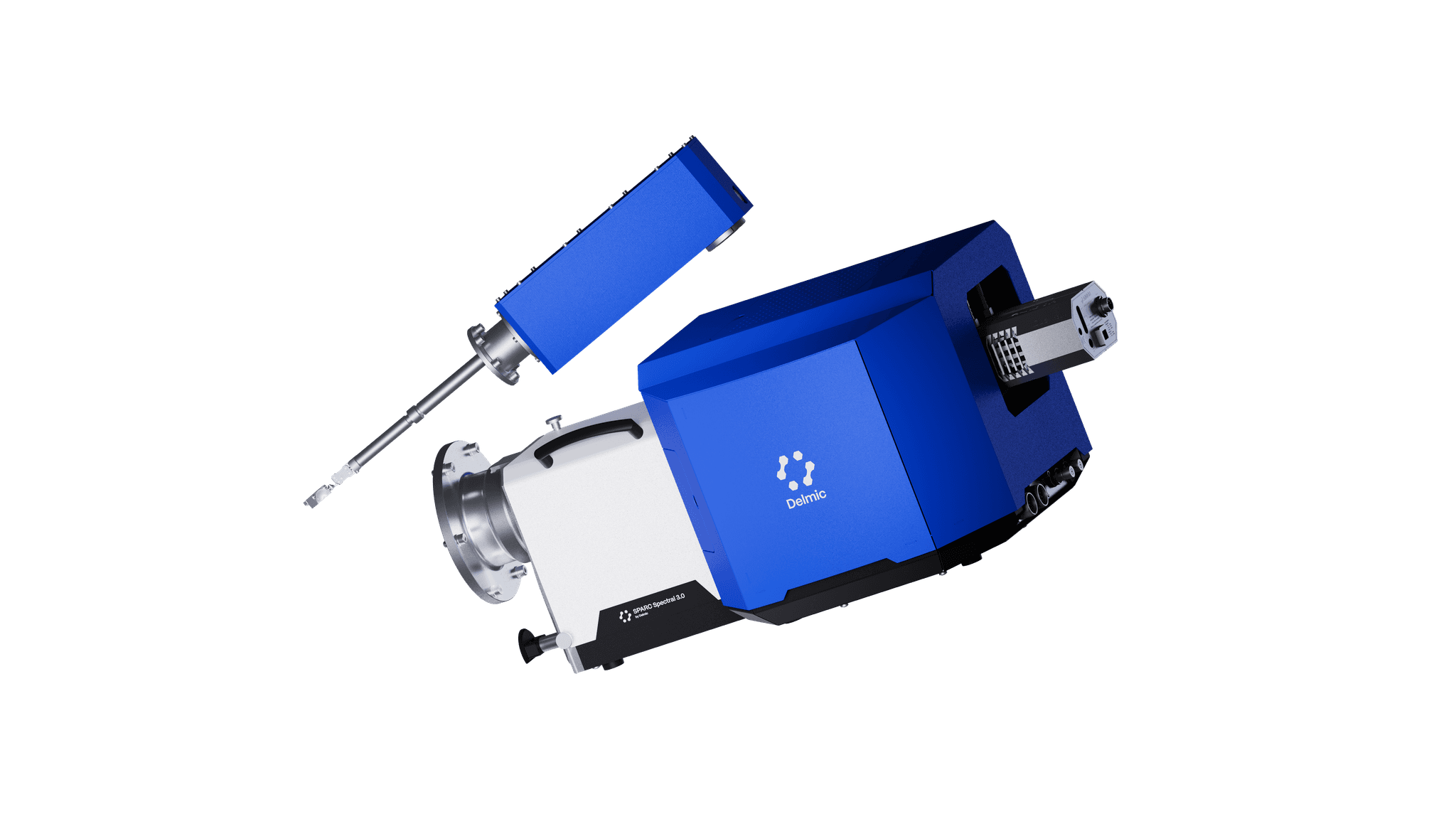
SPARC 3.0
The new measurement system offers several advantages. For one thing, it reduces researchers’ dependence on scarce specialized personnel. This is important, for example, in the semiconductor industry. By 2030, the European semiconductor industry faces a shortage of approximately 10,800 skilled professionals per year. Because the system performs more tasks on its own, even less experienced users can take reliable measurements.
Furthermore, with automatic settings and saved measurement protocols, measurements are less dependent on the person operating the equipment. “In materials research, you want to know whether a difference is truly inherent in the material and not caused by someone having set the device just a little differently,” explains Den Hoedt.
A third advantage is that larger series of measurements are performed automatically in succession, allowing researchers to collect much more data without anyone having to sit at the microscope constantly. This is not only faster but also makes it possible to perform higher-resolution measurements in the same amount of time. With SPARC 3.0, Delmic performs over nine spectroscopic measurements per hour, compared to nearly four with the previous generation.
Finally, SPARC 3.0 has another important advantage: researchers can combine two measurement methods. Thanks to an upgrade, they can direct laser light directly into the electron microscope and measure, at the same location, how a material reacts to both electrons and light. The sample does not need to be transferred to another instrument for this. This enables new experiments involving, among other things, solar cell materials, quantum technology, light-sensitive semiconductors, and photocatalysis.
Accessible to industry
With SPARC 3.0, electron microscopy takes a step closer to industry—exactly what Delmic aims to achieve. Den Hoedt: “Delmic has been in existence for over fifteen years now. We started out in the academic sector, and that was our primary focus until 2020.” More than 220 research institutes in over thirty countries use Delmic technology for cryo-electron tomography, cathodoluminescence, and large-scale electron microscopy.
Den Hoedt continues: “In recent years, however, we saw that there was a clear need in industry for a more accessible and efficient way of working with electron microscopy. Our system allows us to meet that need.” The product has only just hit the market, but Delmic has already received a lot of positive feedback. “We’ve indeed received a lot of feedback that automation is very important and that multimodality—that is, integrating light—is a very useful feature.”
A bright future
Den Hoedt is optimistic about the future. “From 2011 to 2018, we had about 30 systems worldwide. Now there are more than 200 in use.” And the number keeps growing.
The schedule for the rest of the year is already quite full, according to the CEO. “The plan is to sit down with industrial clients. In many ways, this system was built for them. So we have a strong case to make.”