ASML joins TNO’s Eindhoven photonics factory
With the pilot line and ASML’s involvement, photonics in Brainport is moving further from promise to production floor.
Published on June 23, 2026

Bart, co-founder of Media52 and Professor of Journalism oversees IO+, events, and Laio. A journalist at heart, he keeps writing as many stories as possible.
TNO and ASML are joining forces on the new Photonic Chip Pilot Line at the High Tech Campus Eindhoven. The goal: not only to design photonic chips more intelligently, but also to learn how to manufacture them reliably, reproducibly and at greater scale.
The factory is still under construction, yet the next chapter in Eindhoven’s photonics story is already taking shape. TNO and ASML are combining their expertise around the new Photonic Chip Pilot Line at the High Tech Campus Eindhoven. This gives Europe’s ambition for chips that process data with light a very tangible form: the transition from promising technology to a manufacturing process capable of operating at volume.
The collaboration focuses on lithography, process control and metrology. These are precisely the areas that determine whether integrated photonics remains an interesting laboratory technology or can grow into an industry with scale, quality and short development cycles. ASML will deploy DUV and I-Line scanners in TNO’s factory. At the same time, the partnership will create a joint R&D environment in which both parties can develop, test and demonstrate processes.
This is an important moment for a technology that has been discussed with high expectations for years. Photonic chips process or transport information using light rather than solely electrical signals. This offers major advantages at high data rates and with low energy consumption. At a time when AI, data centres, sensing, medical diagnostics, 6G and secure communications demand ever more computing power and data traffic, the pressure is growing to bring alternatives to conventional electronic connections to production scale.
From promising chip to predictable process
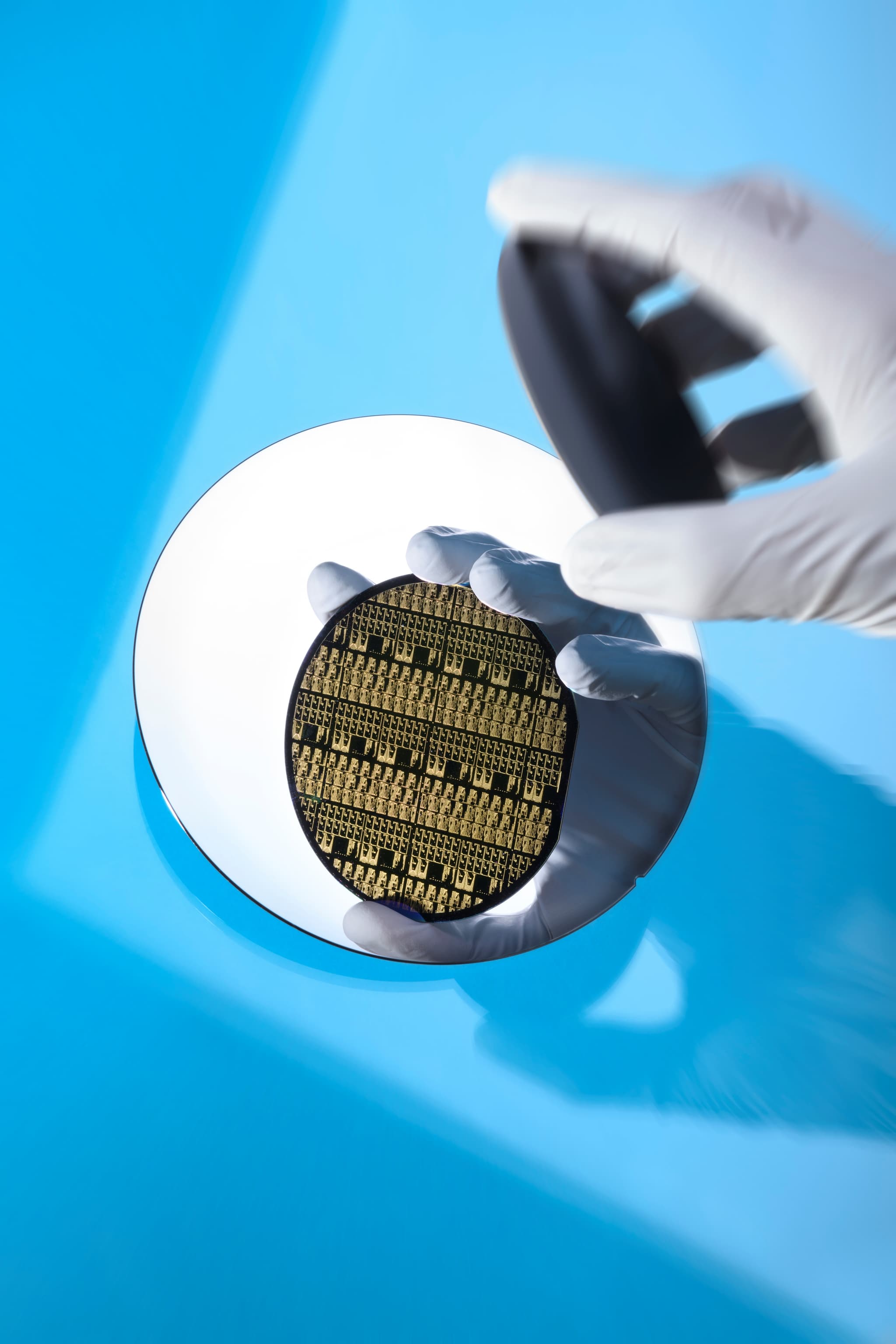
The new pilot line in Eindhoven is designed for photonic chips based on indium phosphide, usually abbreviated as InP. This material is particularly suitable for active functions such as lasers and fast modulation. As a result, InP plays an important role in applications where light must not only be transmitted, but also generated, manipulated or measured directly on the chip.
Producing a chip involves far more than putting a good design onto a wafer. Processes must be mutually stable, deviations need to be measurable, yields have to increase and faults must be detected early. A small difference in layer thickness, alignment or pattern can have major consequences for the performance of a photonic chip. Anyone aiming for volume production therefore needs equipment, measurement methods and process knowledge that together form a single industrial rhythm.
This is exactly where the collaboration between TNO and ASML becomes meaningful. ASML is not merely supplying lithography systems to the new facility. The partnership is also intended to help refine manufacturing processes for integrated photonics. By bringing equipment, process control and metrology together in the same development environment, the partners aim to shorten the path from experiment to scalable production.
The move from four to six inches
The Eindhoven pilot line will enable the production of InP photonic chips on six-inch wafers. That may appear to be a limited change in size, but for the industry it is an essential step. More chips fit on a larger wafer. This can make production more efficient, lower costs and make it more attractive for companies to bring new applications to market.
The pilot line therefore forms a bridge between research and a commercial factory. Companies, start-ups and knowledge institutions will be able to validate designs, test manufacturing processes and discover what is required to produce a chip concept at greater scale. That role is especially important in a sector with high investment requirements, technical risks and long development cycles.
TNO, Eindhoven University of Technology and the University of Twente are working together on this through the Photonic Integration Technology Centre, PITC. This brings together design expertise, technology development and industrialisation. The collaboration with ASML adds another layer: the experience of a global player in lithography and production processes that are applied at enormous scale in the semiconductor industry.
Arnaud de Jong, managing director of TNO High Tech Industry, sees the collaboration as a building block for new European chip companies. “This partnership with ASML strengthens our ambition to build European unicorns in the chip industry. By combining our R&D capabilities with world-class equipment, we are creating a unique industrial environment that will benefit the entire industry.”
European ambition gains a production floor
The pilot line is part of PIXEurope, a European programme intended to narrow the gap between research, prototyping and industrial production of photonic chips. For Europe, this is about more than economic opportunity. Photonics touches technologies that are becoming increasingly strategic: AI infrastructure, data communications, defence, quantum technology and medical applications.
Europe wants to become less dependent on manufacturing capacity and expertise elsewhere in the world in these fields. That ambition is only credible when new chip technologies do not remain confined to isolated demonstrators or specialised laboratories. Standard processes, testing facilities, suppliers, design expertise and production lines are needed that connect with one another.
In Eindhoven, this infrastructure is taking shape step by step. The construction of the pilot line was already a clear signal that the region is aiming for a European position in integrated photonics. ASML’s arrival makes that commitment more operational. The question now is: how do you make a photonic chip deliver the same performance every single time, at a price that opens up new markets?
According to Stanislas Baron, senior vice president at ASML, this transition is decisive. “Scaling photonic chip technology requires a seamless transition from pioneering research to volume production. By integrating our lithography systems into TNO’s factory, we are bridging that gap.”
For Eindhoven’s photonics ambitions, that may be the most important message of all. The technology has already demonstrated its potential. The coming years will be about yield, reliability, cost and capacity. With the pilot line and ASML’s involvement, photonics in Brainport is moving further from promise to the production floor.