
AlixLabs wins €2.5 million EIC grant for chipmaking innovation
Sweden’s AlixLabs receives EU backing for its APS™ technology, which makes semiconductor manufacturing cheaper and more sustainable.
Published on November 20, 2026

Team IO+ selects and features the most important news stories on innovation and technology, carefully curated by our editors.
AlixLabs, a Swedish deep-tech company based in Lund with an office in Eindhoven, has been selected for a €2.5 million non-dilutive grant through the European Innovation Council (EIC) Accelerator program. The company could also receive up to €10 million in equity investment from the EIC Fund. The selection underscores the commercial potential of AlixLabs’ Atomic Pitch Splitting (APS™) technology, which could strengthen Europe’s strategic position in the global semiconductor industry.
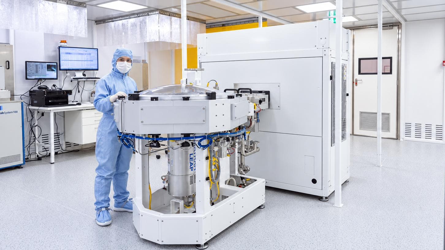
AlixLabs’ APS™ technology is a cyclic plasma-based dry etching process that splits nanoscale structures with atomic precision. It uses Extreme Atomic Layer Etching (ALE) to divide existing nanostructures into smaller features without additional lithography masks or EUV exposure steps. This doubles pattern density while reducing the number of process steps, lowering the cost per wafer, increasing throughput, and cutting energy use, water consumption, and emissions. The technology complements existing patterning techniques such as DUV, EUV, SADP, and SAQP and offers a simpler, more cost-effective approach to advanced chip manufacturing.
Validation on imec’s NanoIC pilot line
AlixLabs is currently testing APS™ on the NanoIC pilot line at imec, a leading European research centre in Leuven. The technology is being evaluated using industry-relevant 300 mm silicon wafers and Intel FinFET test structures. The process has already reduced the half-pitch from 25 nm to 12.5 nm, demonstrating its scalability. Imec prepares and characterises line-and-space structures before sending them to AlixLabs for APS™ process development. The results are assessed against key metrics including critical dimension, uniformity, line-edge roughness, and stochastic defectivity. This validation is a crucial step toward industrial qualification and high-volume manufacturing (HVM).
Strategic support through the EIC Accelerator and Chips Act 2.0
The EIC grant and potential €10 million investment highlight the strategic value of APS™ for Europe’s semiconductor ambitions. AlixLabs is one of 35 deep-tech companies selected from 453 applications, underscoring the technology’s relevance to European technological sovereignty. The selection aligns with the goals of the European Chips Act 2.0, which aims to strengthen Europe’s position in the global semiconductor market. The act includes measures such as faster permitting, support for strategic projects, and efforts to stimulate demand through public procurement of innovative solutions.