
AI is photonics’ killer app. Can chipmakers keep up?
Photonics is limited by supply, not demand. Industry leaders at PIC Summit 2026 explain how to scale chips for AI data centers.
Published on November 18, 2026
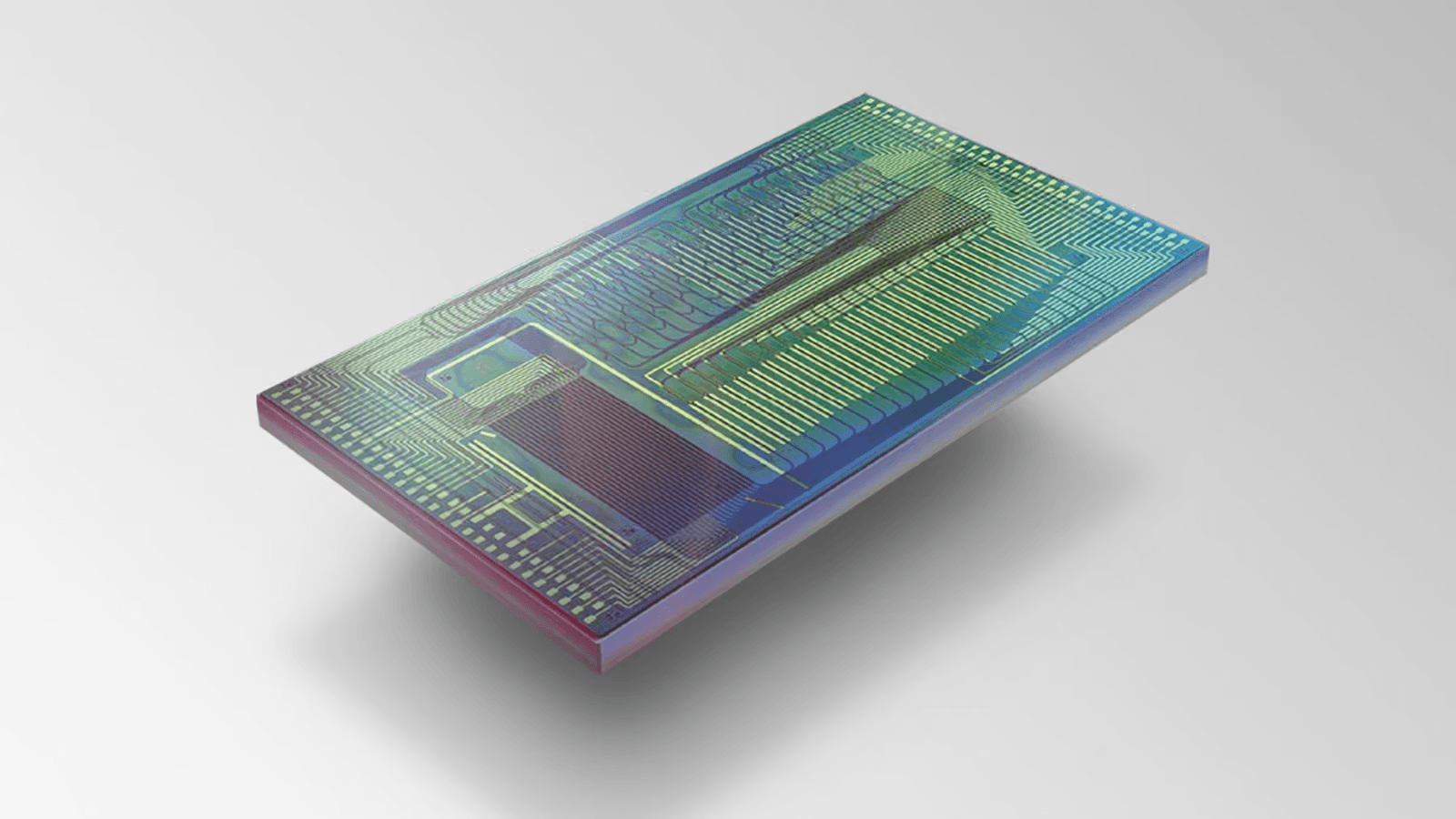
© SMART Photonics

Mauro swapped Sardinia for Eindhoven and has been an IO+ editor for 3 years. As a GREEN+ expert, he covers the energy transition with data-driven stories.
When Johan Feenstra looks back at the first editions of PIC Summit Europe, he remembers an industry still hunting for its purpose. “What’s the killer app? What is going to be the one that actually drives the volumes up for this industry?” the CEO of SMART Photonics recalled. “I think there’s no more discussion about that.”
AI is the answer. The Scaling in Datacom session, held during the event — now in its fifth edition — brought together four companies across the photonics supply chain: foundry SMART Photonics, substrate maker Soitec, optical component giant Coherent and chipmaker STMicroelectronics. Their message was consistent: demand is no longer the problem. The challenge has moved toward securing capacity, integration and industrialization.
Limited by supply, not demand
Feenstra walked through how optics is moving deeper into the data center: from scale-across links between buildings to scale-out links between racks, volumes are ramping up. The industry, he said, is moving from thousands of units to millions, hundreds of millions and eventually billions. Lasers alone are projected to grow by around 50% a year. “I think this growth is even limited by supply, not by demand,” Feenstra said. “If we could supply more, this would go up even faster.”
He also made the case for indium phosphide, the material SMART Photonics is built on, which can integrate lasers, amplifiers, modulators and high-speed detectors on one chip. A year ago, he said, he had to explain to investors a forecast that showed indium phosphide’s market share collapsing. The revised forecast now shows it holding close to half the market and remaining the largest platform into the next decade.
To meet demand, SMART Photonics is contributing to build a 6-inch wafer fab in Eindhoven, with the building due in 2027 and first customer batches in 2028. “This is not a pilot line,” Feenstra stressed. “I can assure you, come and see: this is really a fab.”
Scale also requires partners. Feenstra highlighted a recent collaboration with GlobalFoundries to combine indium phosphide with silicon, and a project with Foxconn announced at the summit. “The end customer cares about one thing only, and that is the specification of the product,” he said. “Whether this is made with one platform or two platforms, they don’t care.”
No single material
For René Jonker, EVP and Chief Product Officer at Soitec, the AI boom is as much a data-movement problem as a computing one. “I would argue the AI revolution is as much about moving data as it is about processing it,” he said, calling connectivity the system’s bottleneck.
No single material can meet every requirement, he argued: silicon scales easily, thin-film lithium niobate enables faster modulators, and indium phosphide makes light sources. The future is “heterogeneous photonics,” combining them on one platform. Soitec’s contribution is engineered substrates: a thin layer of these materials on a silicon base, so they can ride on existing silicon manufacturing.
But breakthroughs are not enough. “It’s one thing to do something once and present it at a conference,” Jonker said. “It’s something completely different if you have to do that millions of times.” Europe has the ingredients, he added, but should learn from Asia’s pragmatism. “Industrialization will ultimately determine who will be the winners in this market.”
Waiting for electronics
Anna Tatarczak, Distinguished Member of Technical Staff at Coherent, put the industry’s progress in numbers. Over two decades, optics has delivered a 150-fold increase in bandwidth density, a 40-fold drop in energy per bit and a 60-fold drop in price per gigabit per second. Yet compute demand is growing about 4.5 times a year while chip performance only doubles, leaving interconnects as the constraint.
She expects many chip architectures to coexist. On speed, she said, photonics is ready for 400 gigabits per lane. “We are waiting for electronics to get there.”
Thermal management is becoming critical next to 1-kilowatt AI accelerators. Her conclusion echoed Feenstra’s: “The manufacturing capabilities do exist, but the market demand now justifies the investment in capacity.”
Betting on 300 mm
Luca Verre, STMicroelectronics’s head of strategy, explained how the chipmaker is returning to silicon photonics. ST began working on the technology about ten years ago for telecom, then parked it because the market was not there. Three years ago it refocused, working closely with key customers and committing “from day one” to 300 mm wafers. “We thought that this market eventually would become a market where scale would be important,” he said. “Those have been important bets we decided to take, which are now paying off.”
The result, PIC100, is now shipping in volume from ST’s fab in France at 200 gigabits per lane, with AWS as lead customer. A next generation aims for 400 gigabits per lane. ST pairs it with its own BiCMOS chips and microcontrollers, because, as Verre put it, scaling optical interconnects is “a system challenge that a company like ST cannot address by itself.”
That was the session’s shared conclusion. Asked where the industry will be in five years, Feenstra expected AI and datacom to remain the largest market, “maybe a hundred times bigger,” with many more applications benefiting once photonics has the capacity, stability, and predictability of a mature industry.